Building a ZX Spectrum Lower Ram Replacement Board - Part 1
As I mentioned in my previous post on messing around with Arduino and 4116 DRAM, the ZX Spectrum is prone to failures of the lower RAM.
Many people (myself included) choose to replace a failed 4116 RAM chip with a modern replacement “board” that uses SRAM instead of DRAM. The reasons are clear, modern boards are made using readily available components - even “new” 4116 chips are all old stock and 30-odd years old. Modern ICs draw less power and importantly drop the requirement for +12V and -5V power lines that the old 4116 chips need.
I’ve bought a couple of these boards myself to repair dead Spectrums. I bought mine from Zigg.net, but there are other people selling them.
Having gone through the Arduino and 4116 project I felt like having a go at making my own would be a fun project.
I’ll spoil it now, I haven’t yet succeeded in making a 100% stable board. But I’m close. This post describes the journey so far.
4116 DRAM - recap
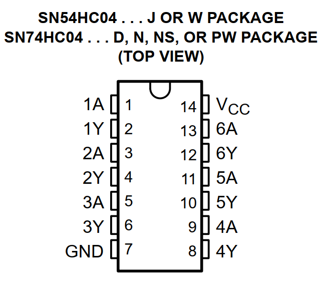
The 4116 DRAM chip is an integrated circuit packaged as a 16-pin DIP.
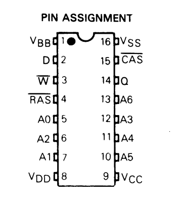
It has 4 pins dedicated to power, 7 pins for addressing, 2 for data I/O and the final 3 are for controlling the chip.
The RAM is addressed with a 7-bit row address and a 7-bit column address, giving 128 x 128 individual “cells” that can be accessed. Each cell has a small capacitance which stores the on/off state of the bit. This is how the memory holds 16kbits of data.
The ZX Spectrum uses 8 of these chips, with each contributing a “bit” of a byte. This is why the base ZX Spectrum has 16K of RAM, it has 8 x 16Kbits = 16k bytes.
In the ZX Spectrum, this lower RAM is shared by both the ULA and the Z80 CPU, but this doesn’t matter for our purposes.
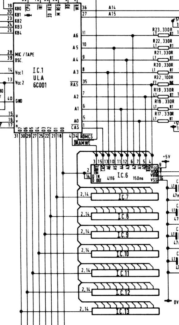
Looking at the
schematic courtesy of
Spectrum for Everyone we can see that each of the 4116 is connected identically except for D, which is the Data In line. The D and Q lines are tied together and connected to one of the D0-D7 I/O lines on the ULA. This works because of how the 4116 itself works; the D and Q pins are used mutually exclusively.
Components - RAM
The first component we need is an SRAM chip. I chose the IDT71256L from Integrated Device Technologies. I’ll be honest and say that I didn’t know if it’d be suitable - and still don’t due to not yet achieving a stable board.
Anyway, the IDT71256L is a 265Kbit (32K x 8bit) SRAM chip. At 32K it’s twice the capacity required for the 16K of the lower RAM, but it’s good enough for us.
I bought the DIP package which has a whopping 28 pins.
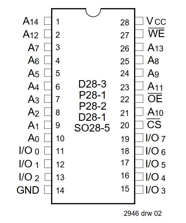
We have 15 address lines, 8 I/O data lines, a Write Enable line and a chip select line. The Output Enable line isn’t needed for us.
The first challenge presents itself. The 4116 DRAM multiplexes the address lines, but the SRAM chip doesn’t. For this, we need a solution…
Components - Logic
If you remember the way the 4116 RAM works with addresses:
- Set the A0-6 ‘row’ address lines
- Pull
!RASlow - Wait for the required interval
- Set the A0-6 ‘column’ address lines
- Pull
!CASlow - Wait for the required interval
We can map this operation onto our SRAM chip by using a flip flop with at least 7 input / output latches.
If we wire the A0-A6 address lines into the flip flop and set them using the !RAS signal then we can then use the outputs of the flip flop as inputs into our “row” lines on the SRAM.
For this I found an octal flip flop in the way of the 74HC374.
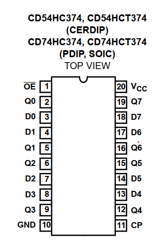
It’s almost perfect for our needs, except that RAS is active low and the chip select on the 74HC374 is active high.
This means I had to toss in an inverter. I chose the 74HC04 - a 14 pin DIP package which has 6 inverters - a bit of a waste but is required.
If I were doing surface mount I could use a single inverter gate, but I’m working with DIP at this point.
With !RAS taken care of, all that remains is to map the column address. This is simply connecting the address lines directly to higher bits the SRAM (I used A7-A13 on the SRAM). We can then pin !CAS to the !CS line on the SRAM. Luckily these are both active low, so they tie together nicely without the need for an inverter.
Here’s the schematic that describes how everything is connected.
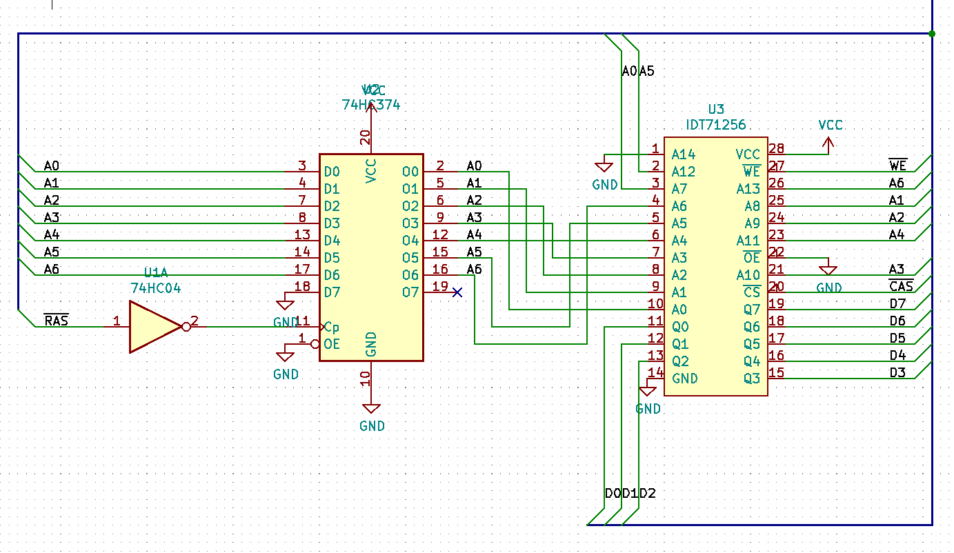
The bus lines lead off to the relevant pins on the ZX Spectrum main board; I used the sockets where I’d removed the original 4116 DRAM.
I don’t think it actually matters which way the address lines get wired, but I went with A0-A6 mapped in order; this does create a crossing rat’s nest of a wire path. I will have to test this at some point.
Prototype v1 - Breadboard
Well actually, two breadboards!
I actually started this journey by poking the SRAM and the logic chips directly with Arduino, mostly to learn how they worked.
The SRAM was hooked up to the Arduino and then I added my flip flop to a second board. It made sense at the time, I guess.
Here’s how it looked:
I originally tested all of this with the 4116 Arduino test library I’d written. I was confident at this point that it least behaved like 4116 DRAM - at least enough to fool the Arduino code.
When it was passing that test there was nothing left to do but to wire it to a ZX Spectrum. I did this by connecting the jumper wires directly to the sockets on the board.
It definitely ain’t pretty. But does it work?
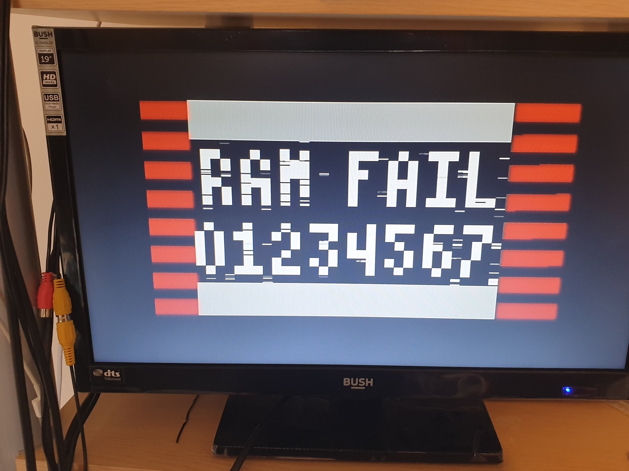
The answer is yes, kinda. It booted to a copyright message, RAMTOP was correct - but the screen was glitchy in the bottom left, like there were errors reading data every now and again. To see what the deal was, I ran it through ByteDelight’s ZX Diag Cart and well, it just said “no”.
Folks on Twitter indicated that it might be due to the wire lengths; there were some HUGE wires on that board and of various lengths too.
Prototype v2 - Breadboard again
The second prototype was basically the same as the first, but instead I used shorter wires. I was a bit excited and in a rush, so I used solid copper core bell wire. It was a bit brittle and broke easily, so was hard to work with.
The next - and biggest problem - was that it was pure white. There’s over 50 wire connections on this board, and when they’re all the same colour one can go a bit snowblind. It made debugging it a pain - and I didn’t have a ‘scope at the time, so I could only do basic continuity tests using my multimeter.
And it failed. Looking back now, the faults look like they’re down to an address line, and possible the !RAS signal, but I had no idea at the time and didn’t really know what to do in order to debug it.
The connections to the board were very loose, and I couldn’t really get that bell wire tight into the socket connections.
Prototype v3 - Breadboard again (again)
I tore out the bell wire and went back to breadboard jumper leads.
TLDR; it failed again - harder than the last time. I did experiment with and without a little “connector” I made by connecting the wires to a socket.
Looking back on this failure, I’d say that the !CAS was failing, as I have since done some experiments as to what certain failures look like. I think I’ll write these up in a later post.
Prototype 4 and beyond
I decided to order myself some stripboard and have a go at making a “real” daughterboard.
Little did I know, this is the point the real ‘fun’ begins.
I’ll write about this little set of adventures in the next part in the series.