Hardware Projects
First blog in a while; I’ve been working away slowly on SMEG but I’ve also been learning how to repair and restore the very hardware I’ve been emulating and writing software for - the humble ZX Spectrum 48K!
I’ll talk about some of the repairs another time, but I thought I’d take this opportunity to write about some of the experiments I’ve been performing with the Spectrum’s RAM.
Why RAM?
Of the two Spectrums I’ve repaired so far, they both have had a failure in one or more of the lower RAM chips (and then an overall failure of the DC/DC converter circuit). One part of the repair of these was to swap out all 8 of the lower 16K of RAM for a “modern” replacement daughterboard. This has left me with 16 chips just gathering dust.
Following the progress of a 4116 RAM tester by a chap called Stephen Vickers on the Spectrum For Everyone Facebook group really piqued my interest. I wondered if I could learn enough to interact with these RAM chips and then potentially verify if they are working or have shorted somewhere. I’m not interested in building a product for sale like Stephen is doing, but I am interested in the learning and practical application of that knowledge.
The ZX Spectrum’s RAM
The ZX Spectrum 48K has two banks of dynamic RAM; the “lower” 16K of RAM and the “upper” 32K. For this post I’m just going to ignore the “upper” RAM completely, and focus on the “lower” 16K of RAM.
The lower 16K of RAM on a ZX Spectrum consists of 8 x 4116 DRAM chips with a 150ns access time.
Each of these 8 chips supplies a single “bit” of a byte at the same memory address, each chip can hold 16kbits each - hence the 16kbytes storage. In practice, it means we have 8 chips all listening to the same addressing and access signals, but their input/outputs are tied to different data lines on the Spectrum’s ULA.
That this means though, is that if a single 4116 chip goes bad, it affects every byte of data in that lower 16K, thus making it impossible to “boot” the computer - depending on the failure of the chip, it can actually lead into a pathological failure of the power circuits, which in turn can cause more failures, and so on. At this point, a repair often mean desoldering all of these chips and replacing with known good, or a modern replacement board.
There are test kits out there (such as the ZX Diag Cart) that plug into your Spectrum and diagnose such faults in-situ; but if you’re in a position like me where you have 16 chips ona workbench with at least 2 faulty ones you can’t really use a cart to diagnose it.
At this point, I decided to learn about what these chips are and how they work. I thought it’d be a good experience to pick up some new electronics skills on the way - but also to help expand my knowledge about the internals of the ZX Spectrum too.
About the 4116 DRAM
The 4116 DRAM chip is an integrated circuit packaged as a 16-pin DIP.
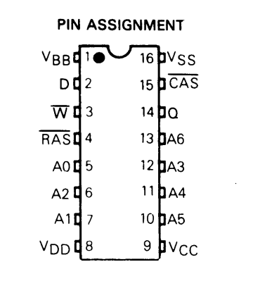
It has 4 pins dedicated to power, 7 pins for addressing, 2 for data I/O and the final 3 are for controlling the chip.
The 4 power pins are a quirky curiosity of the lower RAM in the Spectrum that is not shared by the 4164 / TM4532 / MSM3732 DRAM chips used in the “upper” RAM. This chip requires a +12V, +5V and a -5V line, as well as GND. It is this mix of voltages that makes the chips prone to destroy themselves if they fall out of the tolerance ranges specified.
The RAM is addressed with a 7-bit row address and a 7-bit column address, giving 128 x 128 individual “cells” that can be accessed. Each cell has a small capacitance which stores the on/off state of the bit. This is how the memory holds 16kbits of data.
Internally, it is arranged as two “halves” with rows 0-63 in one side of the chip, and 64-127 held on the other side. This doesn’t materially impact how we interface with the chip, but it does explain some of the quirks of the failures I’ve seen when interacting with the RAM.
As the 4116 is dynamic RAM (aka DRAM) it means that every row must be refreshed every 2ms in order to retain the data; without this the capacitance will leak away and the bits won’t be as you expect them.
Powering up
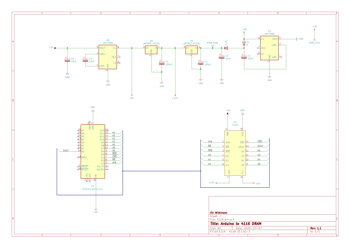
The first problem to solve when wanting to interact with this RAM is how to power it on a breadboard. The real ZX Spectrum has a DC-DC converter circuit that can take the input voltage and output the +12V, +5V and -5V required by the 4116 DRAM; we could try and replicate this on the breadboard, but there’s a much simpler way using a couple of regulators and 7660 charge pumps.
The first problem to solve is getting that initial +12V from the typical +9V DC input. This can be done by using a 7660 charge pump in the following configuration:
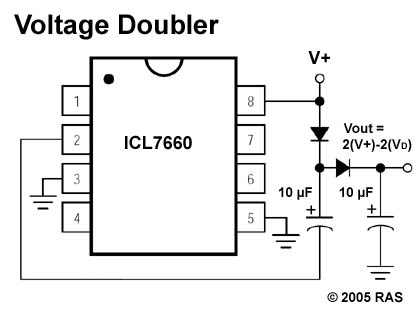
This takes the +9V source and brings it to about +16V after some of the drop off. This is more than enough for our purposes - if we connect that to a 7812 voltage regulator we get a stable +12V. Similarly, the +5V is easy to obtain from either the +9V input, or the +12V line by pushing it through a 7805 voltage regulator.
We now have two of our voltages, what about the third - the -5V line?
This is described nicely on Peter Vis’ site; the solution is a second 7660 in a different configuration.
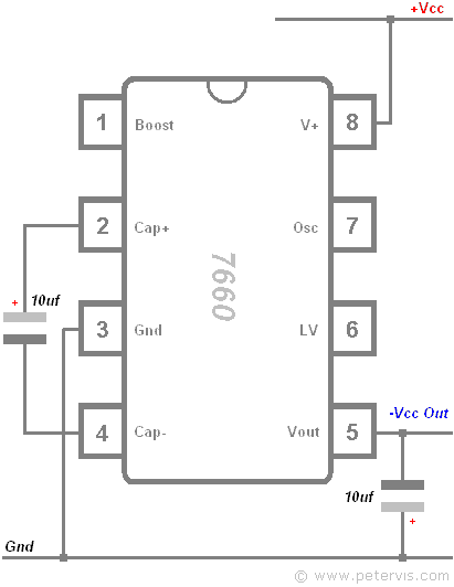
By connecting this to the +5V line off the 7805 regulator, we now get a stable -5V that we can use to power the 4116 chip.
Given we also have a +5V or +9V line we can use that to power the Arduino via the VIN pin (that goes into its internal regulator).
Success! Note - make sure you connect the +12V and -5V lines correctly, I fried a chip because I ran them to the wrong socket pins initially - whoops!
Operating the 4116 DRAM
Now we have power we can get to work understanding what is needed to use the chip itself.
The steps for interacting with the chip are broadly:
- Begin the cycle by ensuring that ~RAS and ~CAS are held high; this generally needs to be for at least the RAS recharge period as documented in the datasheet.
- Present the row address to the A0-6 pins, pull ~RAS low for the required amount of time
- The configuration of the Write Enable (~WE) pin at this point will determine if the operation is a read or a write
- If we are writing (~WE is low), then we should ensure that the data is set on the Data In (D) pin
- Present the column address to A0-6 and then pull ~CAS low for the required amount of time
- If the operation is a read (~WE high), then the data will be available on the Data Out (Q) pin
You’ll see here then that the access address is multiplexed into the address lines. The ZX Spectrum does this by presenting the lower 7 bits of the address first and then the upper 7 bits, thus giving us a 14 bit address (16,384 bits total).
Arduino and 4116
With this in mind, I wired up an Arduino to the various pins and started hacking some code.
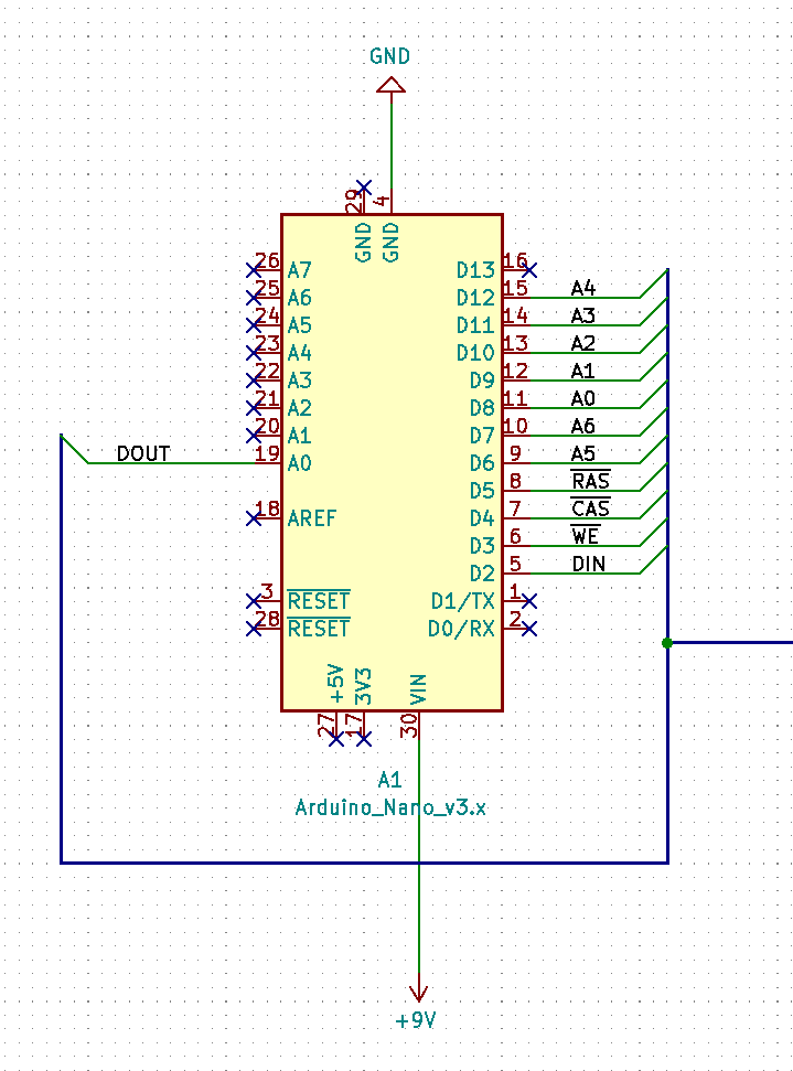
The first “issue” I had was that the Arduino generally works in the order of microseconds, whereas the DRAM is working in the nanosecond scale.
Arduino has a minimum “tick” time of a single clock cycle; to work in orders of nanoseconds (I believe 100ns is the lowest) we burn clock cycles.
To resolve this I used a library by Hans-Juergen Heinrichs that generally gave me what I needed.
The second issue I faced was that I often hit bad reads; after asking on Twitter, I was pointed in the right direction by
@leelegionsmith and
@breakintoprog. I was using digitalRead / digitalWrite from the Arduino library, but they are pretty slow - especially when you need to set a collection of pins at the same time.
The solution was to scrap the friendly helpers and hit up Port Manipulation directly. With this I was able to set all of the address pins in two port writes instead of many individual outputs.
I also made the mistake of using a couple of the “pure analog” pins on the Arduino nano that didn’t exist on the Uno.
This resolved my issue and I was able to start writing bit patterns into the RAM and reading it back out. I’d coded up some simple routines to support the access modes of the RAM. The first two are the classic ‘random’ read/write; the second is the feature that the ZX Spectrum’s ULA relies on a lot for the video RAM - “paged mode”.
The difference between these two modes is really down to the use of ~RAS; you keep it low and then strobe your column addresses & ~CAS signals. This has the effect of being able to read data within the same row much faster than the random I/O. You’re bypassing the extra row address selects and don’t take the hit of the ~RAS recharge time.
Testing RAM
One fun thing here was that I was quickly able to identify “dead” RAM and event deduce the type of failure the RAM has suffered. Some of the RAM just completely failed to be written to; reading it returned the “uninitialized” bit pattern you get when you read new RAM. Other RAM had random bit failures - others had a clear “order” to the failure.
Perhaps I’ll wire all this up into a tester board for myself; perhaps using a Veroboard so it’s a little more permanent than a breadboard!
Learning KiCad
One final thing I did was to start learning how to use KiCad to document the circuits I’ve been building. So here’s the current circuit that’s on the board. There’s probably a few improvements I could make - so feel free to point them out!
So what next?
I moved from here to another ZX Spectrum RAM-related project. Stay tuned for a write up about that soon.