Last time I talked about the beginnings of a project to create an Interak-like VDU for my Z80-based breadboard computer (which is based on the RC2014 bus).
To recap:
- Memory-mapped into the Z80 address space from
$F000to$F7FF - Must be capable of keeping up with least 4Mhz CPU clock
- Monochrome composite output
- Character based, capable of 32, 64 and ideally 80 columns by 24.
- Ideally support “programmable graphics” (custom fonts)
- Based on te Raspberry Pi Pico
I decided that I could achieve memory-mapping by making he Pico a passive bus participant, and effectively “spy” on the writes to the screen RAM. The rest of the system uses it’s main real RAM mapped into that space for reads.
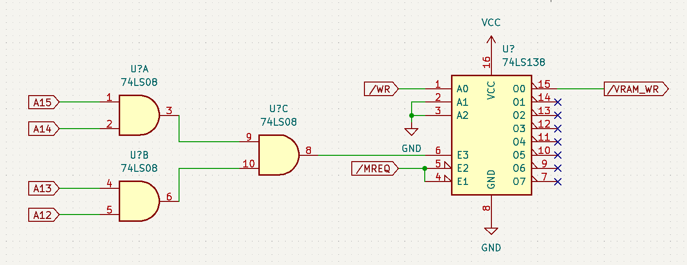
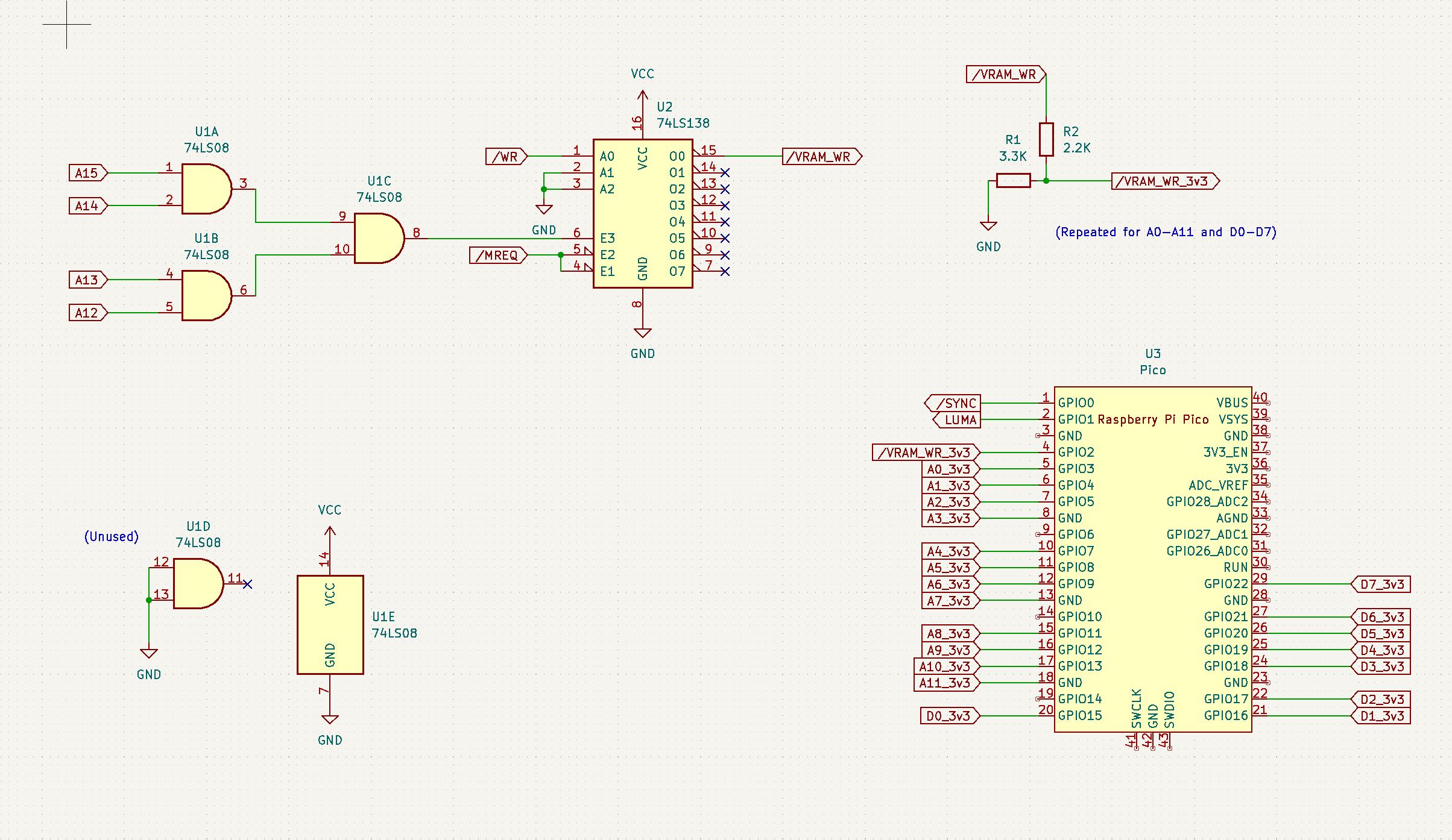
By using some simple electronics based on an 74LS138 and an 74LS08 I could condense 6 signal lines to 1, ensuring it will fit into the Pico’s GPIO count.
Composite out
I’m going to rush through this part a little, but the first thing I did was to sort out the actual composite out. As I’m using monochrome, I can get away with using two wires to drive the required voltages.
The two GPIOs I need are called SYNC and LUMA.
| Voltage Level | SYNC | LUMA | Name | Requirement |
|---|---|---|---|---|
| 0v | LOW | LOW | SYNC | Indicates a sync signal (vsync or hsync) |
| 0.3v | HIGH | LOW | BLACK | This level indicates sync high, and corresponds to the colour BLACK |
| 0.7v | HIGH | HIGH | WHITE | This level indicates sync high, and corresponds to the colour WHITE |
I grabbed Dean Belfield’s excellent Pico-mposite and started exploring it.
Dean’s code is pretty clever and is easy to follow if you know the PAL timings. He uses a PIO with two state machines, both driven by DMA. One state machine is there to drive the sync signals and so encodes the various long/short sync requirements of PAL to indicate hsync/vsync and the back porch.
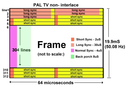
Image Credit: retroleum.co.uk
When it comes to drawing a display line, that kicks off a second state machine which runs at the pixel clock frequency of the display (which differs depending on the resolution). The display line then outputs the BLACK/WHITE voltage levels to emit the pixels themselves.
Dean’s project was designed for greyscale, effectively driving a range of voltages for each shade. I removed the use of multiple pins and tweaked it for my two wire screen. Connecting it up to the TV showed a solid black signal and the TV indicated it was “PAL” format. Good enough for me, so I started drawing some pixels.
Character out
I grabbed the Interak’s CHRAGEN ROM, which contains the pixel images used for the Interak’s display font.
Interestingly, the Interak doesn’t use an 8x8 font, instead it uses an 8x10 font encoded into 2 bytes per character. This means each of my characters is 10 pixel lines high; so with 24 rows it means an effective vertical resolution of 240 pixels.
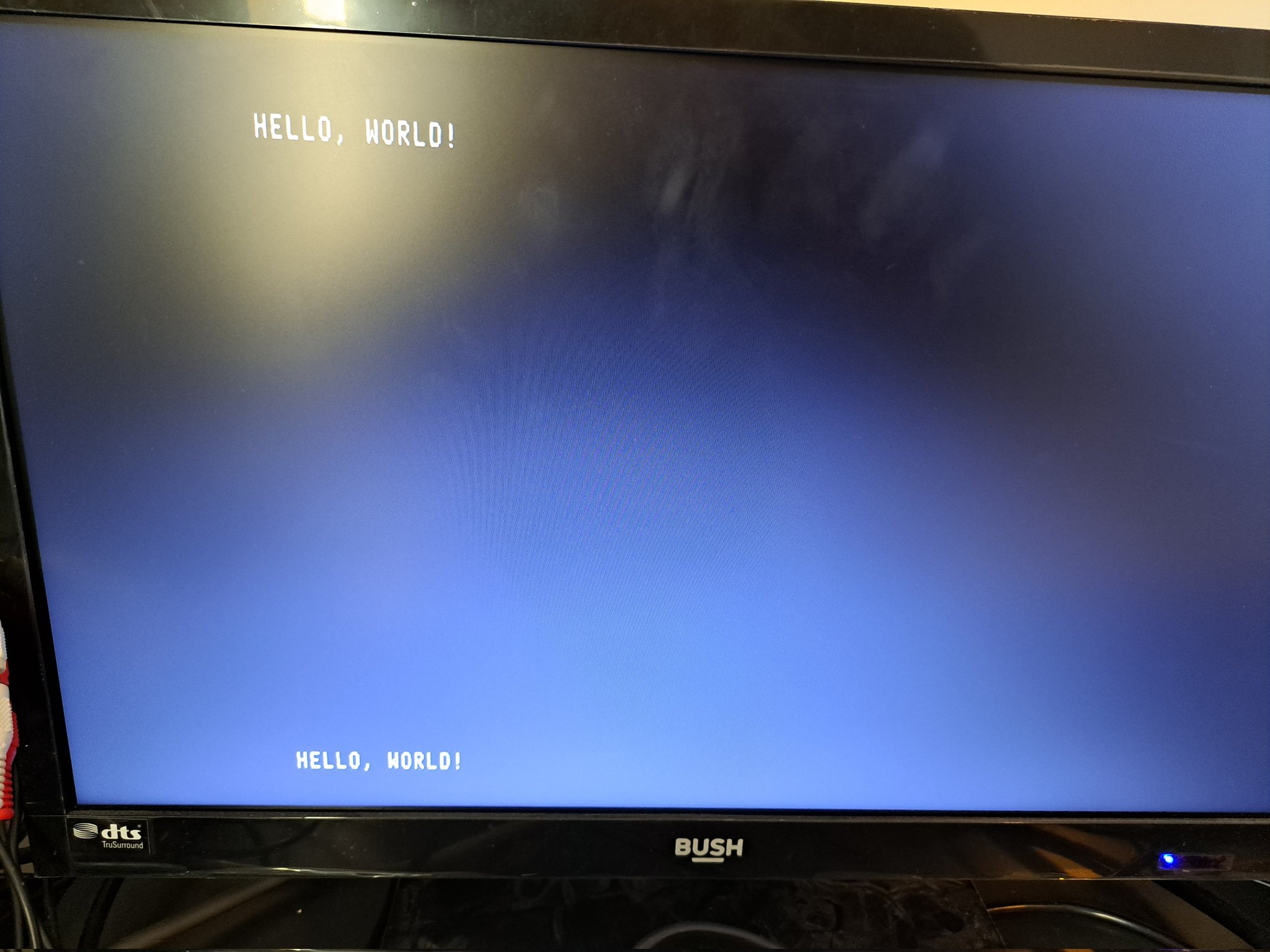
My first approach to outputting the display was to literally create a flat framebuffer in the Pico’s RAM and copy the font’s pixel data to that to display the text “Hello, World!”. This mirrored Dean’s approach and worked initially, I’ll talk a bit later how I had to change this.
I needed a few tweak’s to Dean’s scanline counting to match my Interak’s screen size of either 256x240 or 512x240 depending on whether I was using 32 or 64 column mode. Once that was done, I had a relatively nice pixel display using the Interak’s system font.
Connecting to the system bus
Now comes the interesting part.
The Pico is interfaced to the system bus with 12 address lines, 8 data lines and the /VRAM_WR signal.
I chose to assign the pins as such:
                        PI PICO

                  -------\___/-------
        SYNC  GP0 |  1           40 | +VBUS
                  |                 |
        LUMA  GP1 |  2           39 | +VSYS
                  |                 |
              GND |  3           38 | GND
                  |                 |
    /VRAM_WR  GP2 |  4           37 | 3V3_EN
                  |                 |
         A00  GP3 |  5           36 | +3V3
                  |                 |
         A01  GP4 |  6           35 | ADC_VREF
                  |                 |
         A02  GP5 |  7           34 | GP28  NC
                  |                 |
              GND |  8           33 | GND
                  |                 |
         A03  GP6 |  9           32 | GP27  NC
                  |                 |
         A04  GP7 | 10           31 | GP26  NC
                  |                 |
         A05  GP8 | 11           30 | RUN   NC
                  |                 |
         A06  GP9 | 12           29 | GP22  D7
                  |                 |
              GND | 13           28 | GND
                  |                 |
        A07  GP10 | 14           27 | GP21  D6
                  |                 |
        A08  GP11 | 15           26 | GP20  D5
                  |                 |
        A09  GP12 | 16           25 | GP19  D4
                  |                 |
        A10  GP13 | 17           24 | GP18  D3
                  |                 |
              GND | 18           23 | GND
                  |                 |
        A11  GP14 | 19           22 | GP17  D2
                  |                 |
         D0  GP15 | 20           21 | GP16  D1
                  -------------------
The idea being that the GPIO pin increases as the bit number gets higher, so reading D7-D0 would result in the correct bit order when read by the Pico.
It’s crucial to remember that the Pico is a 3v3 device, so directly wiring it up to the 5v RC2014 bus is a no-no. I decided to use a simple voltage divider to drop the 5v signal to 3v3 (3.3k and 2.2k Ohms). Unfortunately this meant using 42 resistors to cover the whole bus, phew. You can (and probably should) use a dedicated line level converter for this number of lines.
With this connected up to the Pico it was time to start looking at code.
VRAM Write
The first thing to do was to code up the PIO code to handle the signal from the system bus.
To achieve this, I mapped the GPIO 2-21 as inputs in my state machine and then coded it to watch for the active low /VRAM_WR signal.
.program system_bus_vram
    wait 1 pin 0    ; wait for /VRAM_WR high (system boot)

.wrap_target
    wait 0 pin 0    ; stall until the /VRAM_WR is LOW
    in pins, 21     ; read all of our pins
    push            ; send to fifo rx
    irq set 0
    wait 1 pin 0    ; wait for the /VRAM_WR to go high
.wrap
This code simply stalls until the right signal is seen, then pulls the state of all the pins, sends them to the RX buffer and fires an interrupt.
The interrupt code that runs on the ARM is equally as simple:
void sysbus_vwr_irq() {
    io_rw_32 *rxfifo_shift = (io_rw_32*)&pio_system_bus->rxf[sm_sysbus_vram];
    while (!pio_sm_is_rx_fifo_empty(pio_system_bus, sm_sysbus_vram)) {
        unsigned int pins = *rxfifo_shift;
        if ((pins&1) == 0) {
            const uint addr = (pins & 0b111111111111) >> 1;
            const uint data = (pins >> 13) & 0xFF;
            vram_wr(addr,data);
        }
    }

    if(pio_interrupt_get(pio_system_bus,0))
    {
        pio_interrupt_clear(pio_system_bus, 0);
    }
}
Its job is to read the RX buffer, decode the address and tell the vram there’s been a write.
I coded up some Z80 code to run on my breadboard machine, essentially writing to screen memory at a fixed location.
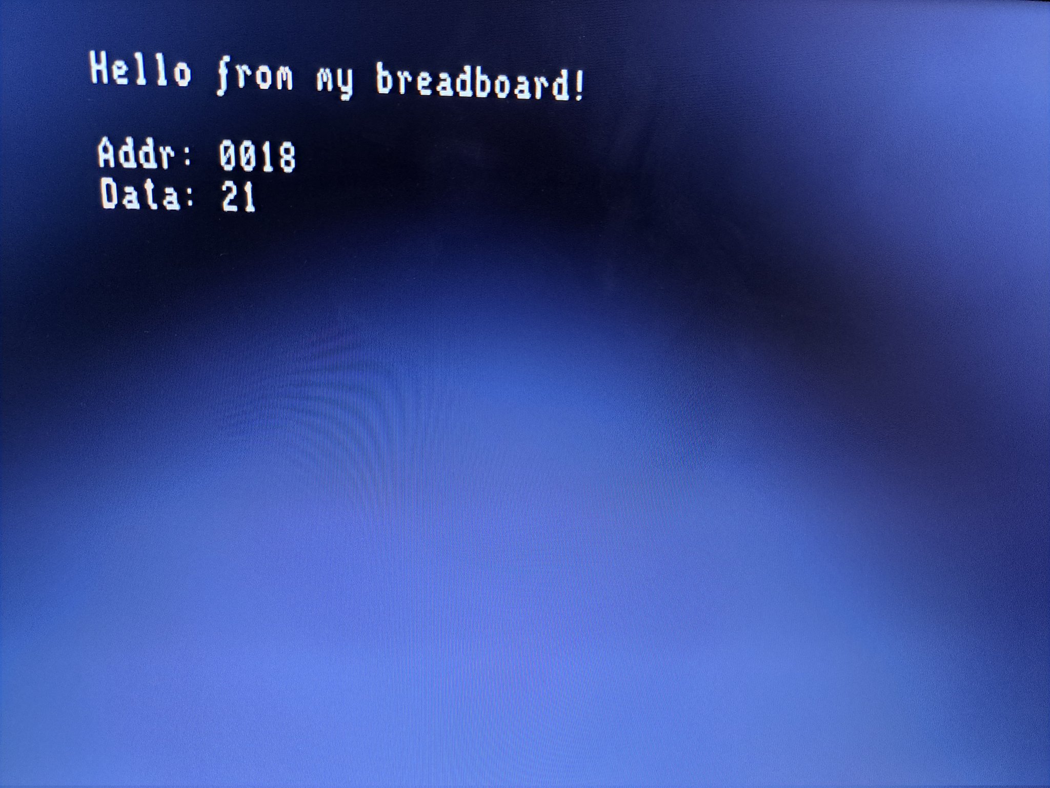
For testing, I made the screen output a message with the 12 bit address and the data it saw. In this example, only the address and data lines come from the Z80, the rest was hard coded into the Pico.
Full screen
Now I know the Z80 can send data to the Pico, it’s time to start using this to make a display.
I coded the Z80 to write out a string.
    ld de,msg
    ld hl,$F000
loop:
    ld a,(de)
    or a
    jr z,end
    ld (hl),a
    inc hl
    inc de
    jr loop

end:
    jr end

msg:
    db "Hello, World!", 0
I changed the Pico side rendering code to emit the character into the framebuffer when it saw the write.
This was essentially:
- use the character code as an index into the
CHARGENrom data (code * 2) - enter a 10 pixel line loop
- write out 8 bytes into the framebuffer based on whether the pixel is
1or0 - increase the pixel line, loop
I found that this worked, but I was missing characters. The code that ran in the interrupt was too slow to happen in the interrupt itself and as a result, the RX buffer filled up and caused data to get lost.
This became more evident when I wrote a simple two phase clear loop that:
- looped from
$F000to$F600(64 cols x 24 lines) - wrote
#to each location - looped again, this time writing
If this was fast enough, you’d see maybe a brief flash of # on the screen, before it settled to a blank screen.
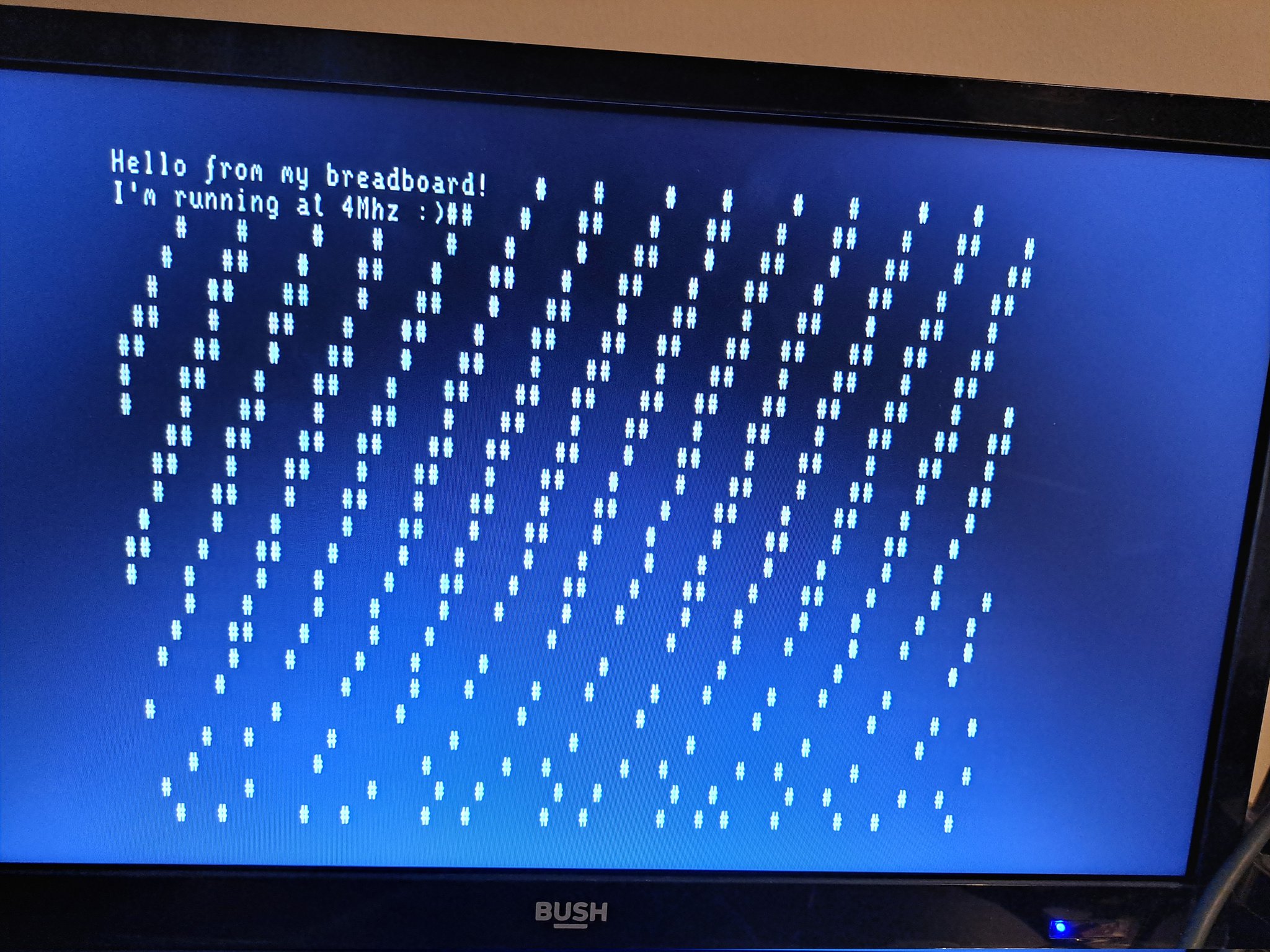
Yup, it clearly wasn’t fast enough at 4Mhz. If I slowed the CPU clock down it would happily work, so I knew it was down to the Pico side and not the Z80.
Simple enough to fix, I thought, but it did mean reworking the rendering code. I changed the vram_wr code to do nothing other than put the character data byte into a 2k byte array which represented the VRAM area; essentially a small mirror of what the Z80 would see.
Optimizing the display generation
The rendering code then had to change; I puzzled about how to do this for a while. A few solutions such as maintaining a delta list and updating it in the Pico’s CPU loop were discarded; instead I chose to drop the idea of a framebuffer entirely and render each scanline on demand.
So I changed the Pico code to fill a scanline buffer for the DMA before it send the data to the state machine.
This worked in terms of all the data showing up from the Z80 (yay), but meant that the extra time to render the scanline caused artifacts in the pixel output.
So I realised, the scanline data needs to be available ahead of time for the DMA to send, and that the generation of the data for the scanline takes more than one scanline.
I ended up creating a buffer of odd/even scanlines that I’d flip between and fill before presenting it to the DMA. Unfortunately, this also wasn’t fast enough. So I made that buffer deeper; 10 pixels deep in fact, to account for a whole character row.
I now dedicated the entirety of core 1 to filling these buffers ahead of time, starting the fill process when the DMA was about half way through the 10 pixel buffer. So essentially there’s a rolling window where the DMA is pulling from the buffer to send to the PIO, and the CPU is filling in behind it.
    while(1) {
        int line = new_line_needed;
        if (line >= 0) {
            new_line_needed = -1;
            draw_screen_line(line+0, line_data_buffer_0);
            draw_screen_line(line+1, line_data_buffer_1);
            draw_screen_line(line+2, line_data_buffer_2);
            draw_screen_line(line+3, line_data_buffer_3);
            draw_screen_line(line+4, line_data_buffer_4);
            draw_screen_line(line+5, line_data_buffer_5);
            draw_screen_line(line+6, line_data_buffer_6);
            draw_screen_line(line+7, line_data_buffer_7);
            draw_screen_line(line+8, line_data_buffer_8);
            draw_screen_line(line+9, line_data_buffer_9);
        }
    }
The new_line_needed flag is set before the top of display (~scanline 41) and then part way through the DMA handler interrupt.
void __not_in_flash_func(cvideo_pio_handler)(void) {

    if ((pixel_line % char_height) == 8) {
        last_line += char_height;
        new_line_needed = last_line;
    }

    const uint8_t* b = line_data_buffer[pixel_line % char_height];
    ++pixel_line;

    dma_channel_set_read_addr(pios[1].dma_channel, b, true);   // Line up the next block of pixels
    hw_set_bits(&pio_video->irq, 1u);						   // Reset the IRQ
}
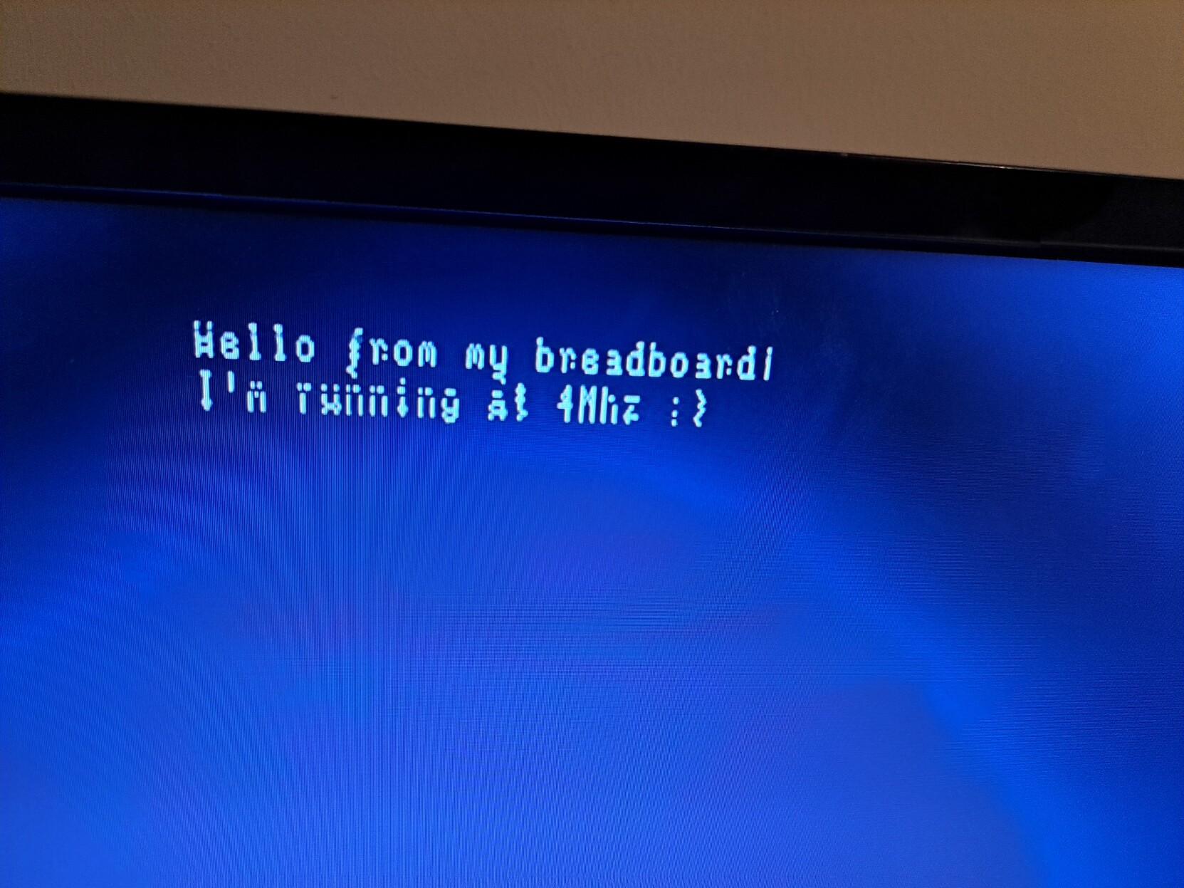
It’s ugly, but it worked. The result was a solid display that was able to keep up with the Z80 running at 4Mhz sending writes in a tight loop (eg: LDIR).
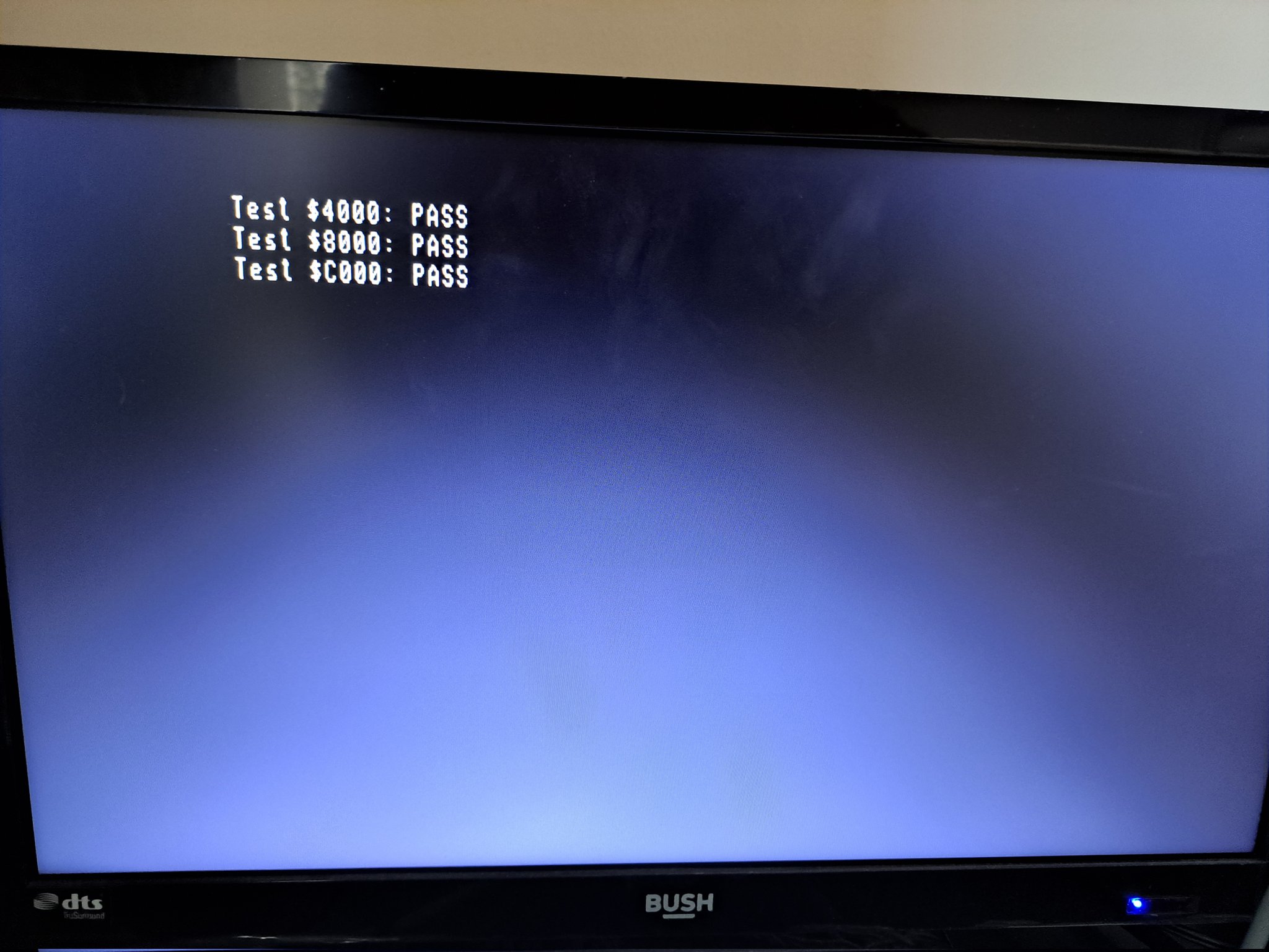
Finally, I was able to actually output directly from the Z80 - so I hooked up some basic diagnostics for the computer to test stuff was actually working.
Recap
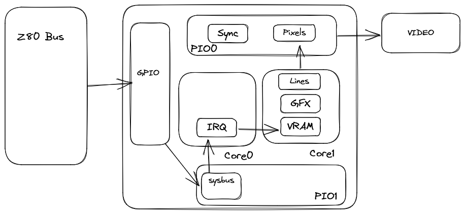
Here’s the rough flow of the components in the Pico and interaction between them.
PIO 0 is dedicated to the composite video output. The main framework of this is based on Dean Belfield’s
Pico-mposite, modified to handle my pixel data and scaled down to two wires, but all of the sync, PIO and dma code is essentially the same. Thanks Dean!
The main loop on ARM Core 1 is dedicated to feeding the line buffers needed by the DMA.
PIO 1 is dedicated to the system bus handling, with the IRQ handlers running on ARM Core 0; as stated before these do very little except “poke” the vram with the right addresses from the bus. The rest of the core is just running with tight_loop_contents() at this stage, but this will change when I move onto the next components.
There’s probably more optimizations I can do here; for example do I need to pre-buffer 10 lines, or can I drop that to 5? Do I need to use the IRQ to signal writes, or can I do that as part of the sysbus main loop? As long as the buffer doesn’t fill, it should be ok. It’s something to look into; but for now it’s a working system and I’m happy enough.
And finally, the electronics part:
Next steps
With all working it got me thinking; can I use the USB port on the Pico to read the keyboard and report this back to the Z80 when it asks for it?
We’ll talk about that in the next instalment.