We took a little detour into the realm of keyboard support for our VDU which would allow it to be part of a terminal system. This time we’re back on the display side, specifically looking at programmable character graphics.
Interak Programmable Character Graphics
Remember that the Interak’s VDU is a text-based display. It deals with taking a screen byte, using it as a lookup into a ROM that contains the pixel data and then outputting it to the screen. However, one of the cards released by Greenbank Electronics in 1982 was the “Programmable Character Graphics” card (or PCG) which promised to provide “high resolution graphics”. In reality, the card allowed the user to customise the bitmap font used for the display e.g: user defined characters which would be displayed on screen instead of the default ROM font. The display was still character-based, but now you can customise the character set.
The PCG card mapped an additional 2K of RAM into the system from $F800 to $FFFF - just after the normal VDU-2K RAM location which could be written to by the user; it’s this RAM location that is used by the PCG card as the source for its pixels.
The mode of operation is pretty simple; if the character in VRAM has bit 7 set then use the graphics from the PCG RAM, otherwise use the normal ROM character. If PCG is not in operation we instead use a pixel inverted version of the normal ROM character when bit 7 is set. Using the PCG does remove the pixel invert mode, but it also means that user defined characters can be used alongside the normal text mode display.
The format of the custom user characters has to match that of the ROM; eg: each character is 16 bytes in size, 8 pixels wide and 10 high.
       7 6 5 4 3 2 1 0
    0: 1 1 1 1 1 1 1 1
    1: 1 1 1 1 1 1 1 1
    2: 1 1 1 1 1 1 1 1
    3: 1 1 1 1 1 1 1 1
    4: 1 1 1 1 1 1 1 1
    5: 1 1 1 1 1 1 1 1
    6: 1 1 1 1 1 1 1 1
    7: 1 1 1 1 1 1 1 1
    8: 1 1 1 1 1 1 1 1
    9: 1 1 1 1 1 1 1 1
    A: - - - - - - - - (not shown)
    B: - - - - - - - - (not shown)
    C: - - - - - - - - (not shown)
    D: - - - - - - - - (not shown)
    E: - - - - - - - - (not shown)
    F: - - - - - - - - (not shown)
Features from the PCG-3
If you remember back to my
Original System vs New School System analysis there are a few subtle differences with some of the behaviours. Having done some analysis of the original circuit board schematics and the new
PCG-3 community designed card, there’s one difference that stands out. The new system responds to a write to I/O port $4E and the original does not.
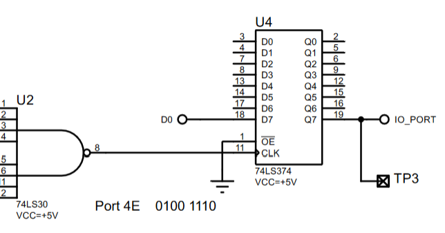
The description on the PCG-3 schematic says:
When (PORT) is high and A11 is low characters are read from EEPROM When (PORT) is high and A11 is high then Prog Graphics are read from 2k of 6164 8K RAM
So essentially, write $01 to port $4E to turn the user defined characters on, write $00 to turn them off.
I don’t believe the original system had this feature; but it seems quite useful to have. Naturally, we’d default to “off” and perhaps later down the line have the ability to toggle it via the port be a VDU settings option.
Implementation overview
This system should be relatively simple to implement. There’s a couple of parts to it:
- The I/O write to port
$4E, set apcg_enabledflag from the data value - Extend the VRAM array in the Pico to 4K in size (
0x1000); allow thevram_wrto write anywhere to it - Update the rendering to use the data in vram at
0x800for the character set if the vram character value has bit 7 set
Part of this would involve writing some more Z80 code to upload the user defined character set and display the full character set.
I/O write handling
This is much simpler to deal with than the reads; it’s a lot more like vram writes in that I can dispatch them to the ARM CPU to decode and handle; as long as it’s quick. If you recall last time, I used a 74LS138 to turn /IORQ, /RD and /WR into 2 signals, /IORD and /IOWR.
                        74LS138

                  -------\___/-------
         /WR    A |  1           16 | VCC   (5V)
                  |                 |
         /RD    B |  2           15 | Y0
                  |                 |
         GND    C |  3           14 | Y1   /IORD
                  |                 |
      /IORQ  /G2A |  4           13 | Y2   /IOWR
                  |                 |
      /IORQ  /G2B |  5           12 | Y3
                  |                 |
         VCC   G1 |  6           11 | Y4
                  |                 |
               Y7 |  7           10 | Y5
                  |                 |
              GND |  8            9 | Y6
                  -------------------
I’ll be using /IOWR here; mapping it to GP27.
                       PI PICO
                 -------\___/-------
       SYNC  GP0 |  1           40 | +VBUS
                 |                 |
       LUMA  GP1 |  2           39 | +VSYS
                 |                 |
             GND |  3           38 | GND
                 |                 |
    VRAM_WR  GP2 |  4           37 | 3V3_EN
                 |                 |
        A00  GP3 |  5           36 | +3V3
                 |                 |
        A01  GP4 |  6           35 | ADC_VREF
                 |                 |
        A02  GP5 |  7           34 | GP28  NC
                 |                 |
             GND |  8           33 | GND
                 |                 |
        A03  GP6 |  9           32 | GP27  /IOWR
                 |                 |
        A04  GP7 | 10           31 | GP26  /IORD
                 |                 |
        A05  GP8 | 11           30 | RUN
                 |                 |
        A06  GP9 | 12           29 | GP22  D7
                 |                 |
             GND | 13           28 | GND
                 |                 |
       A07  GP10 | 14           27 | GP21  D6
                 |                 |
       A08  GP11 | 15           26 | GP20  D5
                 |                 |
       A09  GP12 | 16           25 | GP19  D4
                 |                 |
       A10  GP13 | 17           24 | GP18  D3
                 |                 |
             GND | 18           23 | GND
                 |                 |
       A11  GP14 | 19           22 | GP17  D2
                 |                 |
        D0  GP15 | 20           21 | GP16  D1
                 -------------------
Unlike the vram_wr handling code, we only care about the 8 lower address bits and the 8 data bits.
As I’m decoding the port in the ARM, it gives scope to listen for writes to other ports. This can be useful in the future, for example if I wanted to fake out parts of a 6845 CRTC to switch to the 80 column mode or show a hardware cursor (required by some of the VDU-3 software).
For this work I can just do a simple check for port $4E and set a pcg_enabled flag using the value of the lower bit.
Code wise, it’s pretty simple:
    ; Listens to /IOWR active low
    ; reads pins, dispatches to system
    ; pins mapped
    ;   IN  A7-0
    ;   IN  D7-D0
    ; IORQ pin is GP27 (24)
    .program system_bus_iowr
        wait 1 gpio 27      ; wait for /IOWR high (system boot)

    .wrap_target
        wait 0 gpio 27      ; stall until the /IOWR is LOW
        in pins, 16
        wait 1 gpio 27      ; wait for the /IOWR to go high
    .wrap
I learned that I could use auto-push in the state machine’s settings to simplify things. Essentially, as soon as I push the pins the ISR is cleared and the data is available to the system.
This time around I decided to experiment a little and not use an IRQ, but instead have the state machine’s RX buffer be pulled in the sysbus core’s main loop. It’s not really doing anything except for polling the usb, so it seemed to make sense.
Screen drawing changes
The first change to make is to extend the size of the vram array from 0x800 to 0x1000 and remove the same restrictions from the vram_wr code. The writes to the screen memory can now address the full 4K of RAM.
The scanline rendering code has to change a bit; the pseudocode that follows describes the logic we need:
    if pcg_enabled:
        if char_code >= 128:
            draw char with gfx from vram[0x800] and above
        else:
            draw char with gfx from char rom
    else:
        if char_code >= 128:
            draw char with gfx from char rom but invert pixels
        else:
            draw char with gfx from char rom
I decided to implement this via two standalone scanline draw functions; one for the “normal” mode, the other for when pcg_enabled is set. The rationale for this is that the code is very time sensitive, so I wanted to avoid checks to the pcg_enabled setting during the loop of the scanline creation. I also select the function based on the pre-buffering, so the effect here is that each block of 10 scanlines I pre-render has the same PCG setting.
Z80 code
The next bit to do is write some test code to verify all this works. This is reasonably simple; as it only needs to do a couple of things:
- copy a custom character set to
$F800 - output to port
$4Ewhen it wants to enable it - write characters to the screen with bit 7 set to show the user defined characters
The last point was already done; the ROM I’d written to test the main screen output the whole character set:
    ; print charset
    ld a,0
    ld hl,$F000 + (SCREEN_COLS * 20)

    ld b,0
.putc:
    ld (hl),a
    inc hl
    inc a
    djnz .putc
This code writes 4 rows of 64 characters, covering the whole set.
To upload the data it’s a simple case of writing to the memory; but I needed a character set to test with! Luckily my friend
Sam supplied me with a CHESSMEN ROM character dump from his original Interak system.
    ; upload programmable gfx
    ld hl,chessmen_gfx
    ld de,$F800         ; pcg location
    ld bc,$800          ; 2k
    ldir

    ... snip ...

    ORG $2000
chessmen_gfx:
    INCBIN "chessmen.bin"
And then for testing purposes I modified my key loop to check for the character p, which would then toggle the pcg system on or off by using OUT ($4E).
key_loop:
    nop
    in a,($40)
    bit 7,a
    jr z,key_loop
    and $7F ; remove high bit
    ld hl,last_key
    ld (hl),a
    ld de,msg_key
    ld bc,$0500
    call printstr
    ld de,last_key
    ld a,(de)
    ld (hl),a

    cp 'p' ; pressed p?
    jr nz,.done
    call toggle_pcg

.done:
    jr key_loop

toggle_pcg:
    ld a,(pcg_enabled)
    inc a
    and $1
    ld (pcg_enabled),a
    out ($4E),a
    ret
And with a little bit of debugging on the Pico side, I eventually ended up with a screen that shows the CHESSMEN set and can flip between them with a keypress.
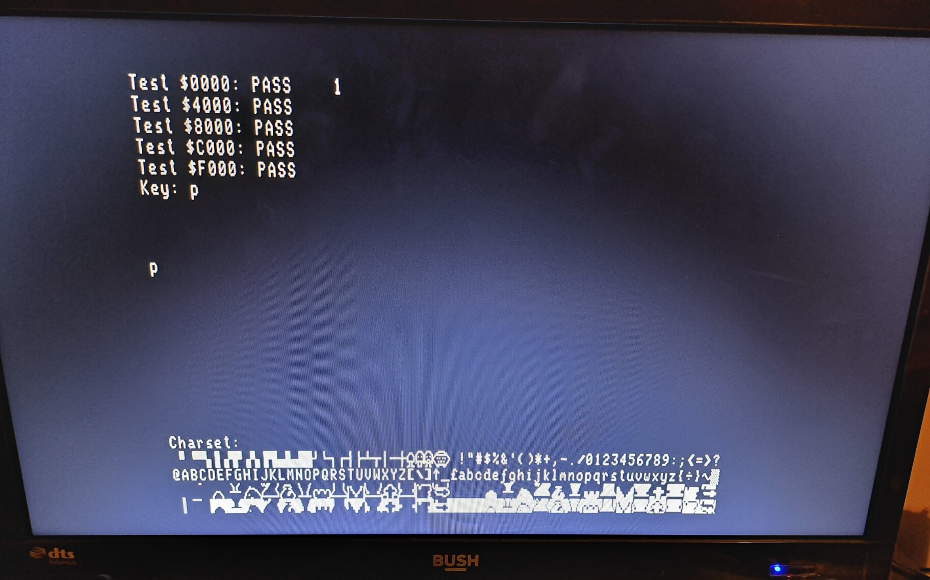
Ignore the stray characters, they’re outputs from the Pico to show the state of things. I’ve said before and I’ll say again, it’s EXTREMELY handy to have the Pico be able to output stuff to the TV - you can dump the state of variables to screen directly. Very handy for inspecting data that comes in from the PIOs!
Wrap up
We’ve got a lot working so far!
Whilst I’d now consider this system to be usable. There’s a few things remaining before I would start to consider this “done”:
- Fix glitches; the display glitches a bit, especially when the usb keyboard is in use. There’s also a slight “shimmer” which indicates the sync timing isn’t exact.
- Finish up the key mapping; I’m not properly handling some of the modifiers as the Interak expects
- An onboard menu system; allow the user to flip between 32, 64 and 80 column modes, turn on/off PCG toggling, etc. This would store the settings in the Pico’s flash.
- Electronics wise, I will look at swapping my 40+ voltage dropping resistors for dedicated line level shifters
- Design a PCB that would fit the RC2014
- Open source the design and code (deliberately not done this until it’s in a human-consumable state)