Some time in late 2020/early 2021 I started a project to build a Z80-based computer on a breadboard. In this post I’ll take a retrospective look at the initial version of the breadboard machine, the motivations for doing it and some of the design considerations. Then we’ll explore the next steps for the project which I am planning on documenting as I go along.
Kit computers
Making your own 8-bit computer seems to be a bit of a rite of passage for people with an interest in old stuff and electronics. It’s easy to understand why - the machines are simple enough to understand and can be built with readily available parts.
It’s something you build with your own hands and can code yourself - in the age of being able to simulate entire systems on a single FPGA, it’s something that appeals to many people, especially those over 40.
Back in the late 70’s/early 80’s it was pretty common to buy “kit computers” for enthusiasts to build and code for themselves. Notable examples from back then are the single board machines such as the Sinclair ZX80 as well as more complex, modular designs like the Interak-1.
The modern era has a plethora of kit computers. There’s recreations of all sorts of machines from the 1980’s. Single board computers are catered for with recreations of ZX80’s (Tynemouth Software’s “Minstrel” series). You can buy fully compatible the ZX Spectrum 128K kits (aka the Harlequin ) and even reproduction boards for the original Spectrum machines.
The hugely popular RC2014 kit does a great job at the “modular” computer concept, providing a backplane and bunch of individual modules that can be assembled to add various functions to the machine. There’s even folks out there making PCBs that recreate the Interak-1.
Kit computers are great as they often come with all the components and some nice step-by-step instructions for how to assemble them. When you’re done there will be some software you can run on them before you decide to explore maybe writing your own. I’ve never built a kit computer, but I do fancy it. It’s like doing an airfix kit without the painting - plus you end up with a computer at the end.
Homebrew computers
Some folks like to go off-piste and build their own machine instead of assembling a kit. Here you’ve got the ultimate freedom but have to figure things out if things go wrong. You’ll have to source your own parts, draw your own diagrams - and likely write your own software, depending how much you deviate from standard designs.
Making a homebrew computer isn’t anything original. There’s a heap of projects out there that are doing the same thing - and that’s great, because it means there’s a lot of information available to help. Reference designs, schematics, ideas - all very helpful when approaching your own.
- Grant Searle’s projects - Grant has a variety of designs - including a CP/M compatible machine
- Dean Belfield’s BSX - Dean’s making an MSX-inspired machine
- The Z80-Mini - A single board Z80 with a UART
- Couch to 64K - Mike Sutton’s “Bread80” machine
- Various Hackaday - Loads of others on Hackaday
I’ll probably keep a running list of interesting projects I find along the way.
Making your own
There’s a few decisions to be made when rolling your own Z80 machine.
The first big decision is around the architecture of the machine. Does it need to be CP/M compatible? Does it have pageable ROM? How much memory does it have? Can you page in more RAM? Lots of small decisions here have repercussions down the line, so it makes sense to know what you’re aiming at. If it doesn’t follow a standard (such as CP/M) then you’re unlikely to be able to run any software that’s not yours. It’s up to you to decide if that’s important or not.
Another decision is whether to go for a single board computer (SBC) design or a more modular one. With single board computer designs you can tie things together pretty tightly (eg: RAM/ROM layout) and provide extensibility for IO by exposing some of the bus for peripherals.
With a modular design you tend to have looser coupling as the system should be able to deal with swapping out modules for different ones and largely keep working. The entire bus is generally exposed for all modules to hook into as they see fit.
If you choose a modular design you’re going to have to decide on the bus layout and how you’re planning on connecting the modules to the bus itself. Do you want to be able to interface directly with common peripherals?
The breadboard machine architecture
When I first started this project I decided that I wanted to simulate some of the features of the Amstrad CPC 464. At the time I was struggling to get hold of a CPC and figured “let’s try and build something that loosely follows that design and see where I end up”. I was (and still am) particularly intrigued by the “write-through” to memory when a ROM is paged. That’s a feature I’ve not seen in many other machines and was something I wanted to play with.
Landing on that design choice immediately gives some kind of structure to the project.
- System clock @ 4Mhz
- 64K RAM
- 2x16K ROMS, pageable into the low (
$0000-$3FFF) and high ($C000-$FFFF) memory addresses
At this stage I’m not going to be considering the other stuff that makes the CPC what it is, specifically the gate array which would be a challenge.
In addition to this I’ll be adding a UART so I can interface the machine to my PC for debugging purposes.
Breadboard overview
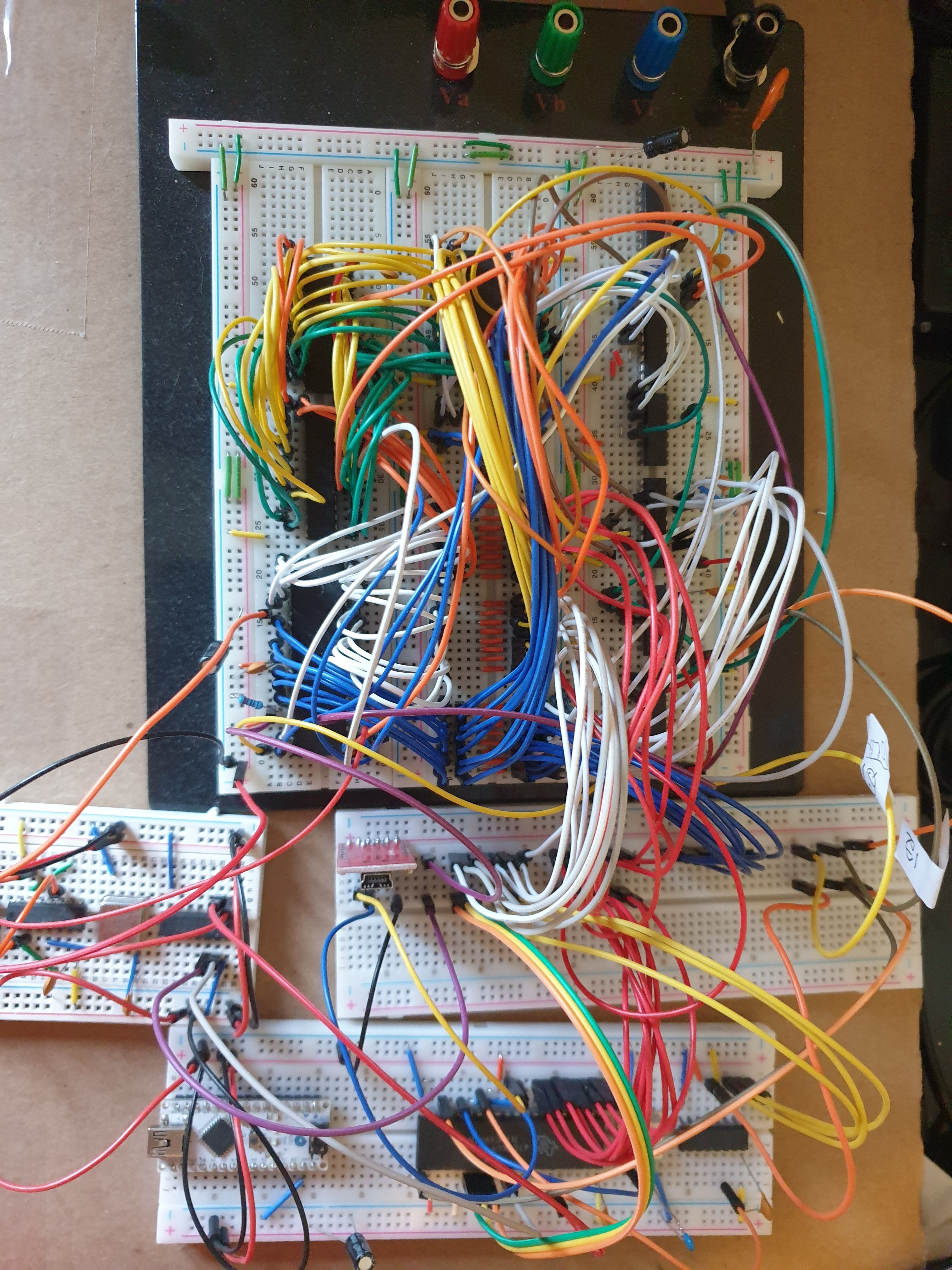
I parked this in late Feb 2021 when life got in the way. Here’s a couple of pictures that show the evolution and main parts.
The board has:
- 16MHz Clock board (divided to 4MHz)
- 2x32K SRAM chips
- 256K EEPROM (single chip)
- Z80 CPU
- Address “decoder” and “RMR” handling (more later)
- 16C550 UART
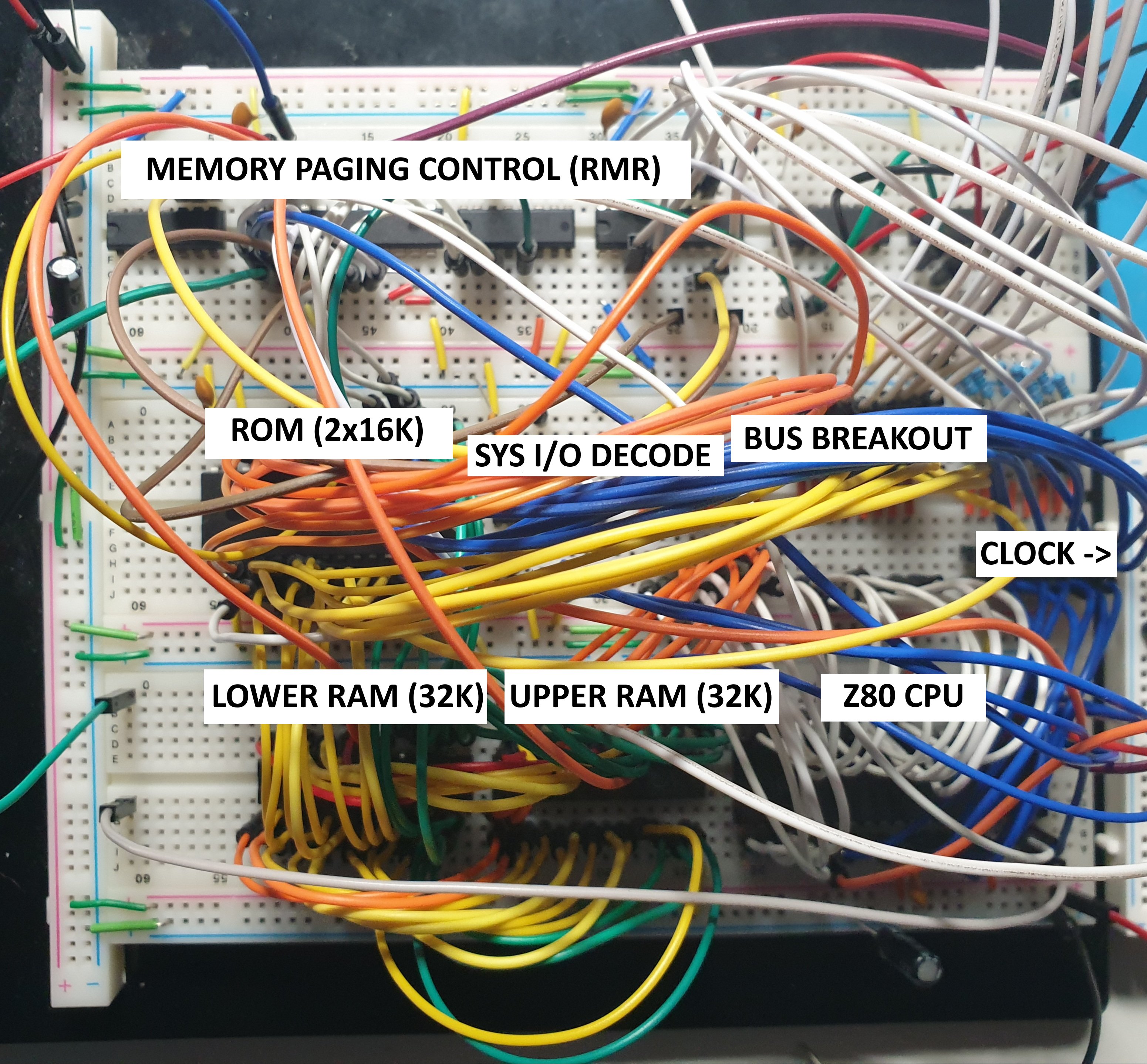
Look at the complete mess of wires.
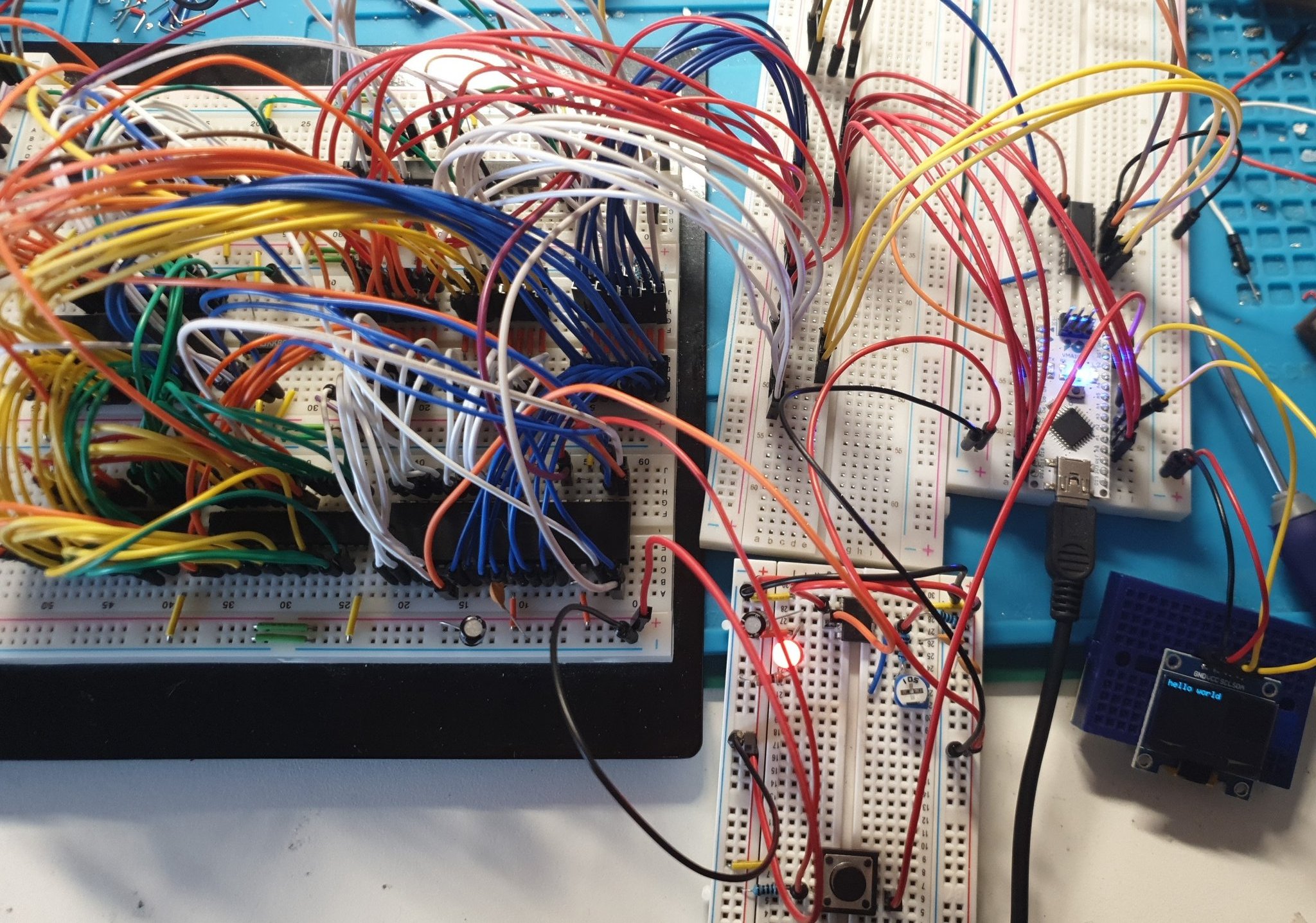
Space got tight, so I dedicated an entire breadboard to the address & data bus.
Pulled out of storage; this shows the dedicated clock board and initial attempts at a UART.
RMR decoding
As I am aiming at a loose CPC464 memory system I needed a way to page in the ROM/RAM. I wanted to use the same ports as the CPC’s gate array (eg, canonical $7Fxx) and handle the command in the same way. On the CPC this is handled by the
RMR register on the gate array.
| 7 | 6 | 5 | 4 | 3 | 2 | 1 | 0 |
|---|---|---|---|---|---|---|---|
| 1 | 0 | 0 | I | UR | LR | VM | VM |
Where:
I: if set (1), this will reset the interrupt counterUR: Enable (0) or Disable (1) the upper ROM pagingLR: Enable (0) or Disable (1) the lower ROM pagingVM: CPC videomode
For this machine we only (currently) care about the UR/LR settings.
There’s a few things that need to happen:
- IO decoding on port $7F - the CPC only decodes A15 and A14 (low, high, respectively)
- dealing with the “command” byte (RMR is
%100xxxxx)
IO decoding can be done easily with a 74LS138; connect lines A15/A14 then tie the final input low (or high), then use the truth table to drive a /GARQ (Gate Array Request) signal.
Similarly the command decoding can also be doing with a 74LS138. The upper 3 bits on the gate array’s data request are the “command”; we an use these directly in the 74LS138 to drive a specific line for further decoding of the command args.
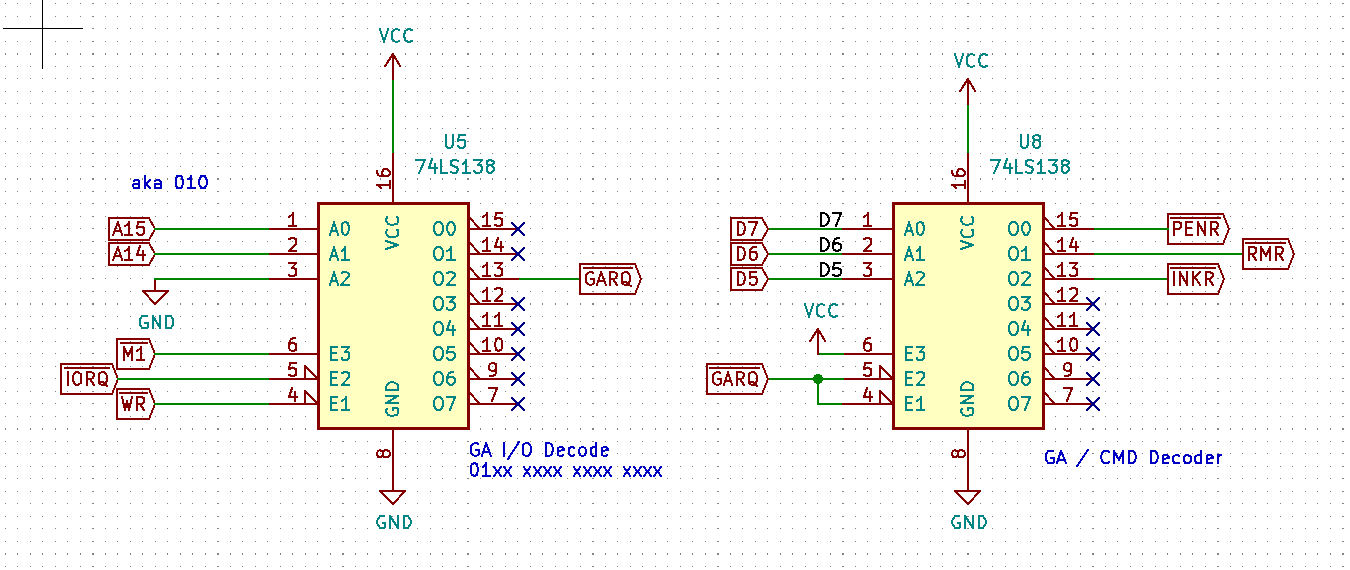
The RMR command is the one we’re interested in so we break that out as an /RMR signal.
RAM/ROM Chip Selects
In order to achieve the CPC’s RAM/ROM paging behaviour we need to describe how it works. I like to start in plain English first:
- If we’re WRITING to memory (
/WRand/MREQactive) then we ALWAYS want to chip select RAM.- Because I’m using two separate 32K SRAM chips, I need to further route this signal to the correct RAM chip.
- If I used a larger RAM chip then I could do away with this, but I only have the 32K chips at this time.
- If the address is between
$0000and$7FFFthen select RAM0 - If the address is between
$8000and$FFFFthen select RAM1
- If we’re READING from memory (
/RDand/MREQactive) then there’s more rules to apply.- If the address is between
$0000and$3FFFAND theLRvalue is 0, then ROM0 is selected - If the address is is between
$0000and$3FFFAND theLRvalue is 1, then RAM0 chip is selected - If the address is between
$4000and$7FFFthen select RAM0 - If the address is between
$8000and$BFFFthen select RAM1 - If the address is between
$C000and$FFFFAND theURvalue is 0, then ROM1 is selected - If the address is between
$C000and$FFFFAND theURvalue is 1, then RAM1 is selected
- If the address is between
Complicated, huh?
When inspecting the address we only care about bits 15 and 14. These map to:
| A15 | A14 | Mask |
|---|---|---|
| L | L | $0xxx |
| L | H | $4xxx |
| H | L | $8xxx |
| H | H | $Cxxx |
This can be boiled down into a truth table:
| /MREQ | /M1 | /WR | A15 | A14 | /UR | /LR | /ROM_CS | /RAM0_CS | /RAM1_CS | Description |
|---|---|---|---|---|---|---|---|---|---|---|
| H | X | X | X | X | X | X | H | H | H | MREQ must be low |
| X | L | X | X | X | X | X | H | H | H | M1 must be high |
| L | H | L | L | L | X | X | H | L | H | Write to $0xxx -> RAM0 |
| L | H | L | L | H | X | X | H | L | H | Write to $4xxx -> RAM0 |
| L | H | L | H | L | X | X | H | H | L | Write to $8xxx -> RAM1 |
| L | H | L | H | H | X | X | H | H | L | Write to $Cxxx -> RAM1 |
| L | H | H | L | L | X | H | H | L | H | Read from $0xxxx, LR paged out -> RAM0 |
| L | H | H | L | L | X | L | L | H | H | Read from $0xxxx, LR paged in -> ROM |
| L | H | H | L | H | X | X | H | L | H | Read from $4xxxx -> RAM0 |
| L | H | H | H | L | X | X | H | H | L | Read from $8xxxx -> RAM1 |
| L | H | H | H | H | H | X | H | H | L | Read from $Cxxxx, UR paged out -> RAM0 |
| L | H | H | H | H | L | X | L | H | H | Read from $Cxxxx, UR paged in -> ROM |
As I’ve got an oversized ROM (256K vs 32K) I’ve “bypassed” the need for further selection because I can just waste the 32K between pages 0 and 1. A simple fix for this is to ignore A15 on the ROM to map calls to $Cxxx down to $4000 (see earlier addressing table). A further improvement would be to allow selectable ROMs (the CPC has a ROM select at port $DF00) or to use jumpers.
I decided that as this logic is relatively complicated we can cut down on the number of chips by using a GAL. I only have the GAL22V10 chips, so there’s a bunch of wasted pins - maybe there’s a future use for them in the ROM select.
RMR latching
Right now we can detect when the RMR command is sent, and select ROM/RAM from the value that is provided. However we’re going to need to latch these values if we want them to persist after the IO request.
This is do-able using a simple 74LS377 octal latch. We only need 5 of the inputs so the rest are tied low (or high, dealer’s choice). It’s the latched values we use to drive the rest of the logic.
Now, one area of complexity here is that we need to account for a default state of at least the lower ROM (it needs to be set to 1 after power on). The 74LS377 will initialize to a random state after power on, so we need to explicitly deal with this with our reset circuit.
I’ve just looked at the schematic for how I dealt with this originally and there’s a couple of flaws. This will be something I need to address going forward; I think it’s probably achievable by ensuring the data bus is pulled up and then hooking the chip select on the latch up to /RESET to initialize it all to 1 after a reset.
Looking forward
The main thing that got in the way of working on the original board was that it became a mass of wires; it became hard to trace debug, make changes or even move without disturbing something on the board.
Every chip has its own pin layout, so tying the lines together became a real chore - the lack of a standard bus format started to hurt. I did attempt to remedy this by breaking out the data/address bus into nicely ordered lines - but it didn’t help much when trying to debug the main mass of wires.
I would like to remedy this situation by adopting a modular board approach based around the RC2014 bus. There’s a few reasons to do this; the main one is that the RC2014 bus is well documented and looks pretty clean. As the bus connection is a 40-pin header, it also lends itself to breadboards and stripboard nicely.
I’ve decided that rather than using breadboards for each module I’m going to prototype them on breadboards first and then commit them to stripboard when I’m happy with them. This removes the wire spam, makes the boards more solid and generally tidies things up a bit. Stripboard can be a major pain in the ass though, so that’s one compromise that I’ll have to deal with. It is, however, a nice mid-step from breadboard to PCB - which is a logical future step.
There’s more benefits to adopting an RC2014 bus, such as allowing me to use RC2014 modules on my machine (such as the CF card) with little issue. I can also look at using my stuff on a RC2014 kit in the future, whenever I get around to buying one.
The original RC2014 bus has a couple of issues with missing Z80 signals, but this seems to be addressed with the “Pro” bus (extended bus), which brings out things like /WAIT and the /BUSREQ / /BUSACK lines. Unfortunately this means that using a stripboard backplane for these modules is impractical; but I’ll just break these out into “top” headers and use jumper wires to connect between the boards.
Future posts in this blog series will be about taking the breadboard mess and breaking it into stripboard modules for use on a RC2014 bus. I’ll probably start a github project for it and chuck the bits in there.
RET